Canon plans to mass-produce nanoimprint lithography tools from 2027 with a Japanese supply chain, offering an EUV complement for some chip layers. The shift carries major geopolitical implications by opening a path beyond ASML.
Canon aims to bring nanoimprint lithography into mass production starting in 2027, backed by a Japanese supply chain. This is not the end of ASML’s monopoly on extreme ultraviolet: in the coming years it will be a complement for memory and for certain layers, not a replacement. The stakes are primarily geopolitical. A commercial route toward finer circuits now exists that does not go through Veldhoven, and Tokyo is gearing it up while continuing to buy the Dutch machines for its own fabs.

Why lithography determines who can make advanced chips
Lithography draws the circuits on the wafer and sets the minimum feature size of what can be built. On an advanced chip, the step is repeated across dozens of layers. Whoever controls the machines therefore controls access to the most advanced nodes.
In optical systems, the limit is written in the Rayleigh criterion:
CD = k₁ × λ / NA
CD is the minimum printable dimension, λ the wavelength of light, NA the numerical aperture of the optics. The process factor k₁ does not drop below 0.25 in a single exposure. To shrink transistors, you can therefore shorten the wavelength, increase the aperture, or push the process harder.
The industry followed the first path for forty years: from the 436 nm of mercury lamps to the 193 nm of argon-fluorine (ArF) lasers. Then it immersed the final lens in water to bring the aperture to 1.35. At that point a single exposure bottoms out at roughly a 38 nm half-pitch. To go further requires multiple exposures: more passes, more masks, more alignment errors.
From here begin the two responses at the heart of this article. ASML shortened the wavelength to 13.5 nm with extreme ultraviolet (EUV). Canon stepped away from optics: it prints the circuit by contact, like a stamp.
EUV and nanoimprint: two four-step chains
The two chains end at the same point: a relief pattern in the resist that guides etching. What changes is where the difficulty lies. For ASML it is in the source and the mirrors; for Canon it is in the physical contact between mold and wafer.
ASML must tame light, Canon must tame contact: two four-step chains
Both chains end at the same point, a relief in the resist that guides the etch. The highlighted step is the most critical of each technique. Tap a step to read the detail.
Sources: ASML and Canon technology notes; TechInsights; SemiAnalysis. '5 nm' and '2 nm' are marketing labels, not measurements.
A warning about names. “5 nm” and “2 nm” are commercial labels, not measurements: in a 2 nm chip the tightest metal lines have a pitch on the order of 20 nm.
ASML’s technology: extreme ultraviolet
EUV is now the reference technique for the finest layers of leading-edge chips, and ASML is the only company that builds the machines. The price of leadership is a complexity that no competitor has yet replicated.
The source
13.5 nm light does not come out of a laser: it has to be manufactured. In a vacuum chamber the machine fires about 50,000 tin droplets per second; a CO₂ laser hits them and turns them into plasma, which emits in the extreme ultraviolet. Production sources deliver about 600 watts.
In February 2026 ASML demonstrated 1,000 watts by doubling the droplet rate. The goal is to move from 220 to 330 wafers per hour by 2030.
Mirrors instead of lenses
Air and glass absorb EUV. The entire optical path therefore operates in vacuum, and instead of lenses there are multilayer mirrors built by the German company Zeiss. The mask, too, is a mirror: it reflects the pattern, which the optics reduce fourfold onto the wafer.
Each mirror reflects about 70% of the light. After around ten reflections, only a small fraction reaches the wafer: this is why the source power determines throughput.

From 0.33 to 0.55: High-NA
Machines in the NXE series have a numerical aperture of 0.33 and resolve 13 nm. The latest, the NXE:3800E, exposes 220 wafers per hour. The EXE series raises the aperture to 0.55 and the resolution to 8 nm: structures 1.7 times smaller in a single exposure.
The downside is an optical system that halves the exposed field: larger chips must be printed in two halves stitched together. To address this, ASML and TSMC have launched an initiative for 12-inch masks, with a pilot line in 2031 and production in 2033.
Adoption is still in its early stages. In September 2026, ten machines were in operation at four customers. Intel has exposed more than one million wafers; Samsung plans volume production in 2028, TSMC in 2030, according to ASML’s earnings presentation of 14 October.
Costs, energy, limits
An NXE:3800E costs about 400 million, according to press estimates. TechInsights estimates power draw of up to 1.17 megawatts for the former and 1.4 for the latter.
There is also a physical limit. At 13.5 nm, each photon carries fourteen times the energy of a photon at 193 nm: for the same dose there are few photons, and their number fluctuates from point to point. This creates random defects, which are mitigated by increasing the dose and thus slowing the machine down.
The most immediate constraint, however, is manufacturing capacity. ASML delivered 44 low-NA systems in 2025 and expects about 65 in 2026, with another 30% in 2027. It acknowledges this will not be enough to meet demand through 2028, and has agreed with customers on price increases for the most critical products.
Canon’s technology: nanoimprint
Nanoimprint (NIL, nanoimprint lithography) does not project the pattern: it prints it. A mold engraved with the circuit is pressed onto a liquid resist spread on the wafer, and the shape is transferred by contact, at a 1:1 scale.
The process, step by step
- An inkjet head deposits droplets of resist on the field to be printed, metering them according to pattern density.
- The quartz mold, which Canon calls a “mask,” lowers onto the wafer and the resist fills its cavities.
- A flash of ultraviolet light, through the transparent mold, cures the resist.
- The mold lifts off, the relief remains, and the machine moves on to the next field.
The method comes from Texas-based Molecular Imprints, which Canon acquired in 2014. Canon added the precision mechanics of its traditional lithography machines.
What it promises
The first advantage is resolution. Without optics there is no diffraction limit: all that matters is how fine the mold is. The FPA-1200NZ2C, on sale since October 2023, draws 14 nm lines, which Canon equates with the 5 nm node. In December 2025 Dai Nippon Printing (DNP) unveiled a mold with 10 nm lines, intended for 1.4 nm-class logic.
The second is power consumption. There is no light source to feed, and Canon claims about one-tenth the energy of advanced optical techniques.
The third is price. The list price is not public, but in 2023 chairman and CEO Fujio Mitarai spoke of “one digit less” than EUV. On top of that, the mold can imprint three-dimensional structures in a single pass, whereas optics require multiple exposures.
Where it jams
Contact is also the problem. A particle trapped between mold and wafer ruins the chip and can damage the mold, which from that point on reproduces the defect with every imprint.
The mold, moreover, is at a 1:1 scale. In optical lithography, mask errors reach the wafer reduced by a factor of four; here they arrive in full. The master is written slowly with an electron beam and the working copies wear out: for Canon’s engineers, extending their lifetime is the next milestone.
Then there is alignment from one layer to the next. Canon measures the offset in real time through the mold and corrects it by deforming the wafer with the heat of a laser. The wafer’s edges, where the rectangular field protrudes beyond the disk, remain the most delicate area.
Finally, throughput: about 25 wafers per hour per tool, around a hundred for a cluster of four, according to SemiAnalysis. Less than half of an EUV machine.
Where it stands
The first delivery after the commercial launch went, in September 2024, to the Texas Institute for Electronics, a research consortium. In 2026 Canon reports that major manufacturers are testing it under conditions that replicate the factory line. An additional machine, shipped in June, has been brought online; the stated goal is production use from 2027.
Customer names are not public, and as of December 2025 no leading foundry appeared to be committed to production volumes. The natural outlet is memory, where layouts are repetitive and defects are tolerated better: Kioxia has been testing the technique for years in Yokkaichi. According to Nikkei xTECH, Canon is working with DNP and Fujifilm to extend it to DRAM and logic.
From Canon’s nanoimprint work it has also derived a second product. It is called IAP and it does not print circuits: it planarizes the wafer with a glass plate, reducing height variations to 5 nm or less across the entire 300 mm disk. It will arrive in 2027 and, operating without fine patterns, is likely the least risky entry route into fabs.
The two techniques compared
They do not compete on the same ground. EUV wins on throughput, alignment, and maturity; nanoimprint on cost and energy.
| EUV (ASML) | Nanoimprint (Canon) | |
|---|---|---|
| Principle | Optical projection at 13.5 nm; reflective mask, 4x reduction | Contact printing; 1:1 scale mold, UV curing |
| Stated resolution | 13 nm (NA 0.33); 8 nm (NA 0.55) | 14 nm lines; 10 nm molds under evaluation |
| Throughput (wafers/hour) | 220 (NXE:3800E); 260 from 2027 (NXE:3800F) | About 25 per station, about 100 per group of four |
| Power consumption per tool | Up to 1.17 MW; 1.4 MW for High-NA | About one-tenth, according to Canon |
| Indicative price | About 400 million for High-NA | Not public; “one digit less” |
| Maturity | Commercial chips since 2019; about 65 tools expected in 2026 | No volume manufacturing; first deployments expected from 2027 |
| Typical use | Critical logic and DRAM layers | Memory, selected layers, 3D structures |
| Weak point | Cost, energy, scarce manufacturing capacity | Contact defects, mold lifetime, alignment |
EUV versus nanoimprint: where each one wins
Pick a metric and hover the bars. Throughput (wafers/hour) — higher is better.
Sources: ASML product notes; Canon and DNP releases; TechInsights (power) and SemiAnalysis (NIL throughput) estimates; press estimates for prices. The nanoimprint power figure is derived from Canon's 'about one tenth' claim.
Where extreme precision is required on every layer, EUV has no mature alternatives. Where the cost per layer matters and the design can tolerate a few defects, nanoimprint has room. The data come from ASML product sheets, Canon and DNP press releases, and the already-cited estimates by TechInsights and SemiAnalysis.
The new plants: what Japan is really building
Japan is not building chip fabs based on nanoimprint. It is building the capacity to produce the tools and the molds; its new advanced chip fabs, meanwhile, are buying ASML’s EUV.
| Who and where | What it produces | Lithography | Status |
|---|---|---|---|
| Canon, Utsunomiya | Lithography tools: i-line, KrF and nanoimprint | Builds NIL | Opened on 30 July 2025; at full capacity in 2027 |
| DNP | Nanoimprint molds with 10 nm lines | Supplies NIL | Mass production from 2027 |
| Rapidus, Chitose | 2 nm logic | ASML EUV | Pilot line active; volume in the second half of fiscal 2027 |
| JASM (TSMC), Kumamoto 2 | 3 nm logic | ASML EUV | Under construction; production from 2028 |
Canon’s factory
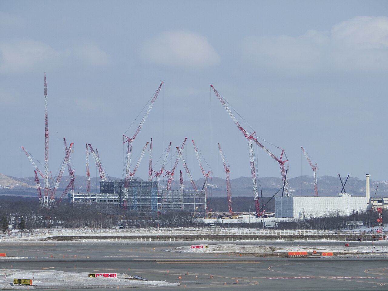
In Utsunomiya, Canon has opened its first new plant for lithography tools in 21 years: about 50 billion yen, 67,500 square meters. Nanoimprint will enter mass production there from the second half of 2027, with a target of ten tools a year by 2028. Since 2021, the technique has also been a research project of the public agency NEDO.

The real volumes, however, are elsewhere. Canon expects to sell 227 lithography tools in 2026 and more than 300 in 2027, almost all i-line and KrF for memory and advanced packaging. These are what finance the bet on nanoimprint.
The state buys Dutch
The government has committed more than ¥10,000 trillion to chips and artificial intelligence by fiscal year 2030. The two flagship projects both use EUV. Rapidus, with more than ¥1.7 trillion in public research funding already authorized, has finalized its process on ASML machines. TSMC will bring 3 nm to Kumamoto starting in 2028, under a plan approved by the Ministry of Economy on 16 October 2026.
The supply chain that already exists
ASML’s EUV already depends on Japan. Tokyo Electron supplies virtually all the tools that coat and develop EUV resist, and Lasertec virtually all the systems that inspect EUV masks. Resist and mask substrates are largely Japanese as well.
Nanoimprint would add the missing piece: exposure. Nikon is also moving, but on another front: by 2028 it is preparing a new immersion ArF platform compatible with ASML machines. It targets DUV, not EUV.
Geopolitical implications
Nanoimprint does not open a back door to China. It does, however, shift the balance of power among allies and offers Beijing a model to emulate.
| Actor | Leverage | Weak point | Recent move |
|---|---|---|---|
| Netherlands and the EU | ASML’s EUV monopoly, Zeiss optics | About 20% of ASML revenue comes from China | November 2025: Dutch controls expanded to the EU list |
| United States | Extraterritorial export rules | No domestic scanner manufacturer | MATCH Act, passed in committee in April 2026 |
| Japan | Resist, masks, inspection; now nanoimprint | Chinese rare earths; Rapidus depends on ASML | Mass-production nanoimprint from 2027 |
| China | Domestic market, rare earths | No access to EUV | EUV prototype, domestic DUV, Prinano nanoimprint |
| Taiwan and Korea | They are the customers: they decide what goes into production | Geographic concentration of fabs | High-NA in production from 2028 (Samsung) and from 2030 (TSMC) |
The bottleneck as a weapon
EUV is the perfect choke point: a single supplier, in a country allied with the United States, and no machines ever sold to China. This is what the architecture of Western controls rests on.
Washington now wants to tighten the screws on the rung below as well. The MATCH Act, introduced on 2 April 2026 and passed out of committee in the House on the 22nd, would ban China from immersion DUV machines and the support for them. The Netherlands and Japan would have 150 days to align; among the targets, according to CSIS, are ASML, Nikon, and Canon.
Its sponsors see it as the last remaining gap: in 2024–25 China imported about 90 immersion tools per year, almost two thirds of ASML’s exports. ASML is opposed. China still accounts for about 20% of its 2026 revenue, and CFO Roger Dassen has warned that new bans would slow Beijing down without stopping it.
Why Canon is not a loophole
Imprint (nanoimprint) machines capable of 45 nm structures or smaller, along with their molds and resins, already appear on control lists derived from the Wassenaar Arrangement. Japan’s 2023 restrictions do not mention nanoimprint, but Mitarai said at the time that he did not consider sales to China to be possible.
What Tokyo stands to gain
Japan is both controller and controlled. It controls materials and machinery without which EUV cannot work. Yet it is also exposed to Chinese leverage: on 6 January 2026 Beijing banned exports of dual-use goods to Japanese military end users, following Prime Minister Sanae Takaichi’s remarks on Taiwan, and rare-earth supplies to some companies were halted.
In this context, a domestic lithography supply chain is worth more than its revenue. It gives Tokyo an alternative to a European supplier whose capacity is sold out through 2028. And it gives Japan one more argument at the table with Washington, where decisions are made about what Canon and Nikon will still be allowed to sell.
What Europe risks
ASML is Europe’s main technological lever, and nanoimprint does not, for now, weaken it. The risk comes from two other directions. The first is dependence on U.S. decisions: the MATCH Act would require The Hague to fall into line within five months. The second is Chinese substitution, which—according to ASML—every new ban accelerates.
Beijing’s response
China is attacking the bottleneck on three fronts. According to Reuters, an EUV prototype has been under testing in Shenzhen since 2025, with the goal of producing chips between 2028 and 2030. Also according to Reuters, a Shanghai state-owned company has started producing immersion DUV machines: about five in 2026, around twenty in 2027. And in August 2025 Prinano delivered the first Chinese nanoimprint machine.
That is the paradox. Nanoimprint dispenses with precisely the two hardest components to copy: the plasma source and the mirrors. If Canon proves it can sustain memory volumes, it will also have shown the way to Chinese manufacturers.
A fragile truce
All of this is unfolding within a provisional trade truce. Between 9 and 10 November 2026, China and the United States extended to 10 January 2027 the suspension of China’s rare-earth controls and the U.S. rule on affiliates. Controls on chipmaking equipment have by now become a bargaining chip.
What changes for the industry
In the short term, nanoimprint will not take business away from ASML. It will reduce pressure on customers who cannot buy enough EUV tools.
Canon itself says so. Mitarai said he does not expect nanoimprint to surpass EUV, and DNP presents its molds as a way to replace “part” of the EUV steps, especially for those who do not have those machines.
The scale gap is stark. Canon is targeting ten nanoimprint machines a year; ASML will deliver about 65 EUV machines in 2026 and, in the third quarter alone, posted revenue of €11.7 billion. Canon’s entire industrial division forecasts 2026 revenue of ¥338.6 billion.
The window nevertheless exists. ASML itself says supply will not meet demand until 2028 and is raising prices. For a memory maker in the midst of an investment race, qualifying a second technique for less critical layers becomes a rational choice.
The target, meanwhile, is moving. ASML is promising 260 wafers per hour from 2027 and 330 by 2030: every productivity gain lowers EUV’s cost per layer and raises the bar for Canon.
Energy remains an issue. An EUV tool draws more than a megawatt. Where the power grid is the constraint on new fabs, a tenth of the power consumption is an industrial argument before it is an environmental one.
For those outside the EUV club, finally, the promise is access. But a lower entry price is not enough: masks, inspection and process recipes are needed—and today those are mature only around Canon.
What to watch
Three signals will tell whether the Japanese bet is working.
A name. The first manufacturer to declare nanoimprint in high-volume production will matter more than any specification. Canon points to 2027.
10 January 2027. The truce between the United States and China expires, and the MATCH Act is not yet law. From then on it will become clear how much room Canon, Nikon and ASML will have left in the Chinese market.
The 2027–28 numbers. Ten nanoimprint tools a year, DNP molds in series production, Rapidus at 2 nm. On the Chinese front, twenty domestic DUV tools and the first chips from the EUV prototype.
The race to 2027: milestones for ASML, the Japanese supply chain and geopolitics
Eighteen dates from the commercial launch of nanoimprint (2023) to 12-inch masks (2031). Filter by actor and hover the dots.
Sources: Canon, DNP, ASML (14 October 2026 results), Nikkan Kogyo, Reuters, CSIS, MLex. Dates from 2027 onward are stated targets, not facts.
Why it matters
Lithography is where chip physics meets industrial policy: today a single European supplier decides who can produce the finest circuits, and the entire architecture of Western export controls rests on that fact. Japan’s nanoimprint wager does not overturn that balance, but it makes it negotiable: it offers memory makers a way out of EUV-tool scarcity until 2028, gives Tokyo one more argument vis-à-vis Washington, and points Beijing to a technical path that skirts precisely the components that are hardest to copy. For Europe, which bases its main technological leverage on ASML, it is a signal to follow closely.
Sources
Main sources, consulted on 10 November 2026.
Canon and nanoimprint
- Canon, Nanoimprint Lithography (technology brief) and interview with developers, 1 October 2026
- Canon, delivery of the FPA-1200NZ2C to the Texas Institute for Electronics, 26 September 2024
- Canon, IAP planarization, 13 January 2026
- Canon, notes to the 2026 earnings presentations: first, second and third quarter
- EE Times Japan, Canon Q3 2026 results, 28 October 2026
- DNP, mold with 10 nm lines, 9 December 2025
- Bloomberg, interview with Fujio Mitarai, November 2023
- Tom's Hardware, analysis of DNP molds and NIL limitations, December 2025
- Nikkei xTECH, nanoimprint toward logic and DRAM, 19 January 2026
ASML and EUV
- ASML, NXE:3800E and EXE:5200B datasheets; 2025 annual report
- ASML, Q3 2026 earnings call, 14 October 2026
- TrendForce via Reuters, 1,000-watt EUV source, 24 February 2026
- Bits&Chips, High-NA availability, 2 September 2026
- Tom's Hardware via TechInsights, EUV tool power consumption
Japanese plants and industrial policy
- Nikkei, opening of Canon’s Utsunomiya plant; Nikkan Kogyo, mass-production nanoimprint from 2027, 19 December 2025
- Jiji, Canon’s production plan for 2027, 21 October 2026
- Semirai, Japanese semiconductor subsidies (Ministry of Economy data), 22 October 2026
- The Register, Rapidus and the 2 nm process, July 2025
- TrendForce, TSMC at 3 nm in Kumamoto, February 2026
- EE Times Japan, Nikon’s strategy on ArF immersion, June 2026
Geopolitics
- CSIS, the MATCH Act and transatlantic relations; China’s rare-earth campaign against Japan
- Bloomberg, ASML’s position on the new bans, 14 October 2026
- Reuters, Chinese EUV prototype, 17 December 2025, and domestic immersion DUV, 28 July 2026
- MLex, extension of the trade truce, 10 November 2026